Raspberry Pi 4 B+ - PCI Express
Connecting external PCI Express devices to Raspberry Pi 4 B+ - since this is the first Raspberry Pi with proper PCI Express interface, it begged to be attempted.

Inspiration
After the daily dose of Hackaday - and with an idea that seemed very doable, and actually, with some improvements can be easily reproducible.
Pi4 - relevant hardware
Without much exaggeration, the new Raspberry Pi is likely the largest single-step improvement on the Pi family since the early changes of the form factor. Although Pi3 introduced 64bit capability, it's been pretty limited in practice due to lack of memory. Pi4 introduces 4GB RAM, USB 3.0 and Gigabit Ethernet.
Most importantly for our purposes, the USB 3.0 (and 2.0) chip is attached via the PCI Express interface - that means, if we were to remove it, we can gain access to the underlying bus. So, without further ado, the sacrificial goat.. uhm, chip.
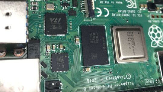
Unfortunately, there is no documentation for the VL805 chip online - only it's bigger (88-pin) cousin VL800. That said, these are sufficiently similar to risk ruining the boards over - and with the visual confirmation over the 3 differential pairs of PCI Express x1 - let's desolder.
Liftoff
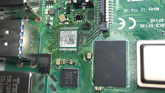
The desoldering is pretty simple - except that the chip has a massive ground pad, which is connected straight to the ground plane of the Raspberry Pi - it required some work with the hot air gun to get it off the board, and I managed to ruin some of the surrounding components. The crocked oscillator above the VL805 serves as the clock for VL805 only - I did end up removing it entirely, but it's not strictly necessary.
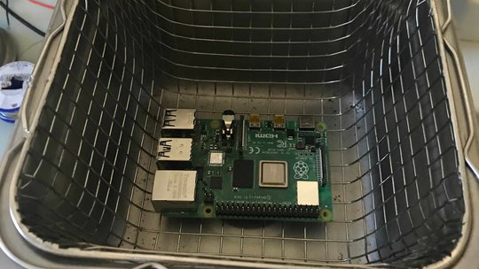
If possible, I'd have wanted to retain the capacitors to the right of VL805 - the next attempt would be much simpler if they were intact. Now, onwards with cleaning!
PCI Express - Theory
PCI Express is a serial bus - which lends itself to relatively few wires. In fact, the entire "data" portion of this hack is done with 6 wires - 3 differential pair.
- Reference Clock - the REFCLK+/REFCLK- pair conveys the clocking information for the bus - from the host to the device
- Lane 0 Transmit - The HSOp(0)/HSOn(0) pair conveys the data (and management information) from the host to the device.
- Lane 0 Receive - The HSIp(0)/HSIn(0) pair conveys the responses from the device (and interrupts, if there are any).
PCI Express - The Riser
This device serves a very simple purpose - allows one to extend the PCI Express bus, and install a device away from a motherboard. This is commonly used if the space, or cooling is at a premium - the devices became very popular in the cryptocurrency mining world, and I've got a few handy.
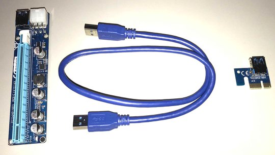
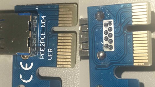
This particular riser takes advantage of a convenient fact, that USB 3.0 cables also use differential signalling across 3 lanes (some use custom cables, some use a pair of SATA cables). This is doubly convenient for our purpose, as it means we can reuse the existing (now defunct) USB 3.0 socket on the Raspberry Pi, and have a detachable PCI Express Bus.
Tracing the Pins
Without the datasheet for VL805, there was still hope in the oldfasioned tracing the pins of the integrated circuit across the board - carefully. An assumption was made (and later proved correct) that the VL800 and VL805 would have the same order in which the PCIe lanes are connected to it - this is easily understood if one considers the silicon design - the die is likely the same, but the packaging differs.
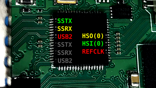
The labels on the USB 3.0 side correspond to the relevant differential lanes in the USB 3.0 connector. The colors represent the lanes that need to be connected to each other - these are most easily obtained by simply tracing the riser itself. As a result, I obtained an almost complete blueprint of what needs to be done.
Capacitors
There is one final peculiarity to pay attention to, before taking out a trusted soldering iron and hoping for a steady hand. To the right of the VL805, and to the left, there are some specs of passive dust - capacitors in 0201 packages, that are critical to the performance of these serial buses.
Both the PCIe and USB 3.0 buses are AC-coupled, that is, there is no direct connection between the relevant chips. This is important to avoid issues around the different bias and drive voltages, as well as allow the system to operate from different power supplies. In short, avoiding the capacitors would lead to non-performance, or even equipment damage.
On the USB 3.0 side, the capacitors are only present on the SuperSpeed (3.0) transmit pair - the other two capacitors should be installed on the device side. On the PCI-Express side, the motherboard is expected to provide this coupling mechanism - the devices expect to be directly attached.
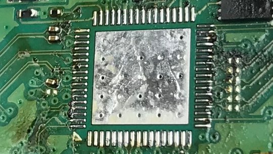
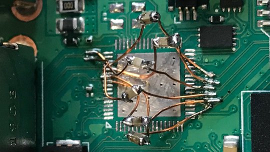
As I have removed most of them during my initial attempts with the hot air desoldering (next time, apply some kapton tape), I'd need to replace these while reworking the connections. Since this is my first attempt and I wasn't sure if I guessed the pairs (and polarity - if it even matters, the PCIe standard allows for lane reversal, but it's unclear if the Broadcom implementation follows this) correctly, I wanted to be able to quickly rewire the interconnect and retry. So the capacitors are all dangling in the air.
I used the 100nF capacitors in a much larger package - mostly to keep them easy to solder - the specification calls for a capacitance between 75nF and 200nF.
Does it all work?
No, not yet. There are few minor details to sort out - the Riser Card uses the remaining 3 wires of the USB 3.0 physical plug (which, in the USB 3.0 standard, are respectively Ground, 5V and Super Speed Ground) for a two of the PCI-Express features: WAKE# (Link Reactivation) and PWRGD (Power Good). This prevents the external card from starting up before the host - and notifies the host that the port is active.
We don't have a need for this feature, and in fact shorting these signals to ground inhibits the card from starting up (it's a likely safety feature to avoid damaging the card if it ends up being plugged in a "real" USB 3.0 port). Cutting the relevant traces, and inserting a 10k resistor fools the card into believing that everything is good.
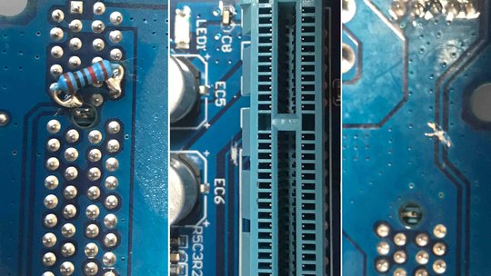
First Light
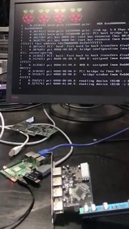
This is actually a still from a slow-mo video of the first boot-up process. Turns out the VIA VL800-based card (oh the irony) doesn't quite like being enumerated by the raspberry pi kernel - it seems that the driver has quirks specifically for the onboard VL805. So the bigger hunt for various controllers begun, culminating with the video/still above.
The subsequent boot of the Raspberry Pi, featuring an Adaptec SAS controller - we can easily see from the LEDs of the controller that it has been initialized by the kernel.
Conclusion
Why did I do it? Because I wanted to see if it can be done. Because Raspberry Pi 4 might be the cheapest device that is PCIe capable after a relatively minor modification (if I didn't lift the capacitors when desoldering the VL805, this is literally 12 soldering points). That, in turn, can be quite handy for developing own PCIe cores for various FPGA based experiments.
I'm sharing it to allow people to learn from this - and to dispel the myth that PCIe is somehow out of reach of hobbyists due to some concerns over signal integrity or complexities. Stay tuned for more Pi4/PCIe experimentation!
